Chips And Smoke

By: Hak8or

Scavange Forum

      With Sparkfun's massive “Freeday” becoming more popular every year, more and more people get access to materials they normally wouldn't be able to afford or have not considered worth the price. The last Freeday went along something along the lines of spending hours on the computer filling out captcha's with the futile hope that eventually, after pressing the submit button, instead of having another captcha on your screen, a gift certificate pops up. After spending nearly six hours on the computer furiously filling out captcha's a $100 gift certificate popped up. After debating the purchase of a large assortment of various doodads or a single expensive item, I eventually reached the conclusion that the coupon should be spent on a hot air station. After a few days, the box was sitting in the basement waiting to be used for the next project.

      Never having used a hot air station before, my garbage bin grew bigger and bigger, containing charred boards, PCB's with bubble on them, and IC's that were burnt to a crisp. From frustration of constant hot air failures, I decided to devote an entire day to de-soldering what ever I can get my hands on with this new hot air station. The goal was not just to get new chips, but also gain some experience, and decrease the size of ever growing junk bin. In the end I had tons of new goodies that I can use for future projects, such as some good RAM IC's, voltage regulators, FLASH memory, inductors, and even a few odd components that just looked interesting.

Desktop

      To start off, this is one of the first desktops I ever found, and the first of many "paces of junk" according to a select few, that took up a large amount of space. It does still work, but the motherboard can only hold slot A processors, which is basically limited to a Pentium 3, four DIMM's of DDR2 ram, a few IDE cables, and a bunch of other standard ports. This is a huge object taking up a large amount of space, sucking a huge amount of power for the performance, and is in general very slow for what I want to use it for, so it is of no use to me. The drawings on the case are from many years ago when I was considering building my own CO2 laser. The CO2 laser was never built due to lack of money for a vacuum pump, not knowing enough about high voltage back then, and lacking the necessary skills for working with glass, but it is still in the back of my mind.

      The object on left is the Xray machine I took apart and posted here a while ago. The computer was thrown away in the end without bothering to scavenge anything as it was getting late in the day, and I already have an entire drawer dedicated to motherboards waiting to be gutted for parts or just thrown away.

Adaptec AHA-2940 PCI-to-Fast SCSI

  • Before

  • Front Side

  • Components

      First up in my list of items which I can dispose of is an Adaptec SCSI card that goes into the PCI slot. Amazon Link It is used as an adapter for an SCSI drive to the PCI slot if your motherboard does not have an on board SCSI port, which was very often the case. Anyways, I don't have any SCSI drives and nearly all fast consumer drives out there now a days run using Sata 3, so this is safe to dispose of. First items that seem to be of interest are the oscillator (never can have enough oscillators,) the LED, a few Dallas chips with large pin spacing, some headers, and what seems to be a shunt resistor to the next to the diode on the far left. Surface mount capacitors and resistors are not really worth taking because you can buy them online from sites such as Digikey or Mouser for very cheap with the exact specs you need instead of working around your limited selection of scavenged ones.


      First de-soldered chip is a DS21S07A from Dallas Semiconductor. It is a couple of termination resistors with some control logic in one IC used for SCSI termination. Although it was not designed for this, it can possibly be used as a couple of controllable pull down resistors for data or control lines. Off the top of my head I cannot really think up of much uses for this chip, but the chances of finding a application for this in the future are high, so this will be kept in a drawer somewhere and eventually be forgotten about anyways.

      Next up is a ST93C46, or according to the chip itself, C46CM1. It is a 1 Kbit EEPROM that is able to be organized as 64 addresses each with 18 bits of storage, or 128 addresses with 8 bits of storage by holding the ORG pin high or low. The package is very simple, with just eight pins, and the interface seems similar to SPI but I see no mention of SPI in the data sheet, regardless there is a clock pin, data in and data out, Chip select, the ORG pin, and the usual power and ground pin, with this being a 5v part. It does register above 3v as logic high on the input though, so you can use your standard PIC's with 3.3v IO, but logic high on the output is VCC, in this case being 5v, so you would need a voltage translator or even a simple resistor divider for transmitting from this EEPROM.

      Lastly, there was an ASIC on the board by Adaptec, probably just serving as the SCSI to PCI converter. Next to it was a 40 Mhz oscillator, which I was unable to find any data sheet for, and a 4 pin male header. A standard red led was also found, not much needs to be said about that. I was unable to find the resistance of the current shunt (metal tab) nor any data sheet, but it will still be kept. The few chips that have stickers on them are most likely ROM's, and will be looked at closer at a later time.

Asus P2898-XV

  • Before

  • Components

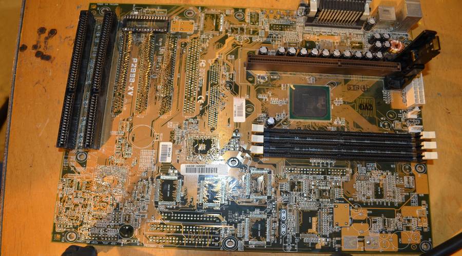
      Now a goodie, a large old motherboard. It was partially already de-soldered because a long time ago when I first got the hot air station I used this board to get an idea for what air pressure and temperature to use when hot air de-soldering, so a few IC's and connectors are already missing. The main purpose for getting parts from this motherboard was because it had large BGA's and even larger connectors, such as the PCI and ISA slots, all of which serve as a fantastic starting point for working with more difficult components.

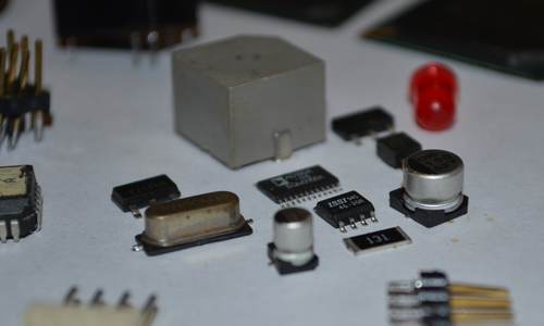
      In the end, I got two quad OR gate IC's, a 40 MHz oscillator, a switching voltage regulator with its two 30V 10 mOhm N channel Mosfets, an inductor, a integrated GPU, and a few other small stuff. Some of the chips I was not able to find much information on either because the chip did not have enough identification marks, the datasheet was proprietary information (ATI integrated GPU), or I just couldn't find the datasheet. It was still a good learning experience to de-solder all these IC's, and the voltage regulator is something I am excited to possibly use for any future projects.


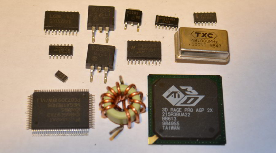
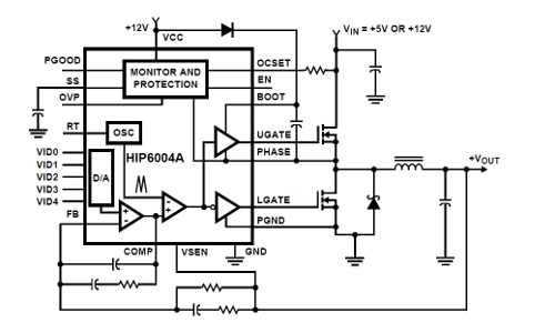
      As processors chug a large amount of power, even the old Pentium 2's, a voltage regulator is needed on the motherboard. Using a linear voltage regulator would be extremely inefficient because these processors are designed to operate at under two volts while pulling a large amount of current, upwards in the 20's. Somewhat recent processors, such as the Q6600 or Pentium 4 required from 60 to 100 amps at a voltage of 1.4 when running at stock. A linear voltage regulator would have to take the lowest voltage rail with a large amount of current capability, such as the 12v rail, and then have to lower that to 1.4 volts while supplying 60 amps, effectively turning it into a nice space heater. Due to this, buck switching voltage regulators are used, which have a much larger efficiency at large currents than linear voltage regulators, often times running with multiple phases to give the lowest voltage ripple, faster response time to constantly changing current demands, less strain on each inductor and mosfets, and power dissipation being more spread out.

      In this case, it is a single phase, synchronous, buck switching converter. The large amount of capacitors are for keeping the voltage ripple as low as possible, and acting as decoupling capacitors for the processor located in the green slot towards the top. Generally, as the current demand increases, voltage ripple required to be lower, or switching frequency is lower, the amount of capacitance needed increases. The copper wire looped around a gray ring is used as the inductor for the switching converter.

      This being a switching synchronous buck voltage regulator means it uses two mosfets (2SK2885), often two N-Channel mosfets, as the switches to connect ground and VSS to the inductor. These mosfets must have low RDS-ON (resistance when fully on) and low gate capacitance to decrease transition times to keep power dissipation as low as possible, especially when dealing with such a large amount of current. You can easily see which of the pins are the gates for each mosfet by the thin trace connected to it.

      The voltage regulator (HIP6004A) is a normal run of the mill chip in this category except for one item. You can control the output voltage using voltage identification pins. These are five pins which are pulled up or down, controlling what voltage the internal DAC creates, which is then sent to a comparator, basically determining what output voltage you want. Five pins allow for 32 steps between two voltages, with the ten lowest steps disabled, enabling you to control the voltage in 0.1v steps for 2.1v to 3.5v, and .05v steps for 1.8v - 2.05v.

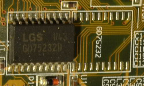
      The GD75232D is a RS-232 transceiver, containing transmitting and receiving drivers. It is used for translating the voltage between the external RS232 12v bus and the internal, much lower voltage bus, as providing protection against ESD and noise on the external bus entering the very delicate circuits of the computer. Not much else needs to be said about this IC. Drivers and receivers are commonplace for external buses, and can be found on every computer which employs such buses.

      Looking closely, you can spot a second spot for another transceiver not occupied. This is a sign that this board may have had different versions being sold using the same PCB in order to save costs, with one of the differentiators being more serial ports. This can be seen in nearly all electronics today, such as phones being shipped with different amounts of storage for different prices but otherwise remaining identical.

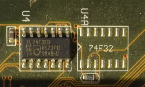
      The TL74F32D is a quad OR gate logic IC. Not much to say since this is a standard logic chip, it runs on five volts, and the datasheet has only three pages for the actual ic itself, with the remaining three pages either mostly empty or meant for sale information. You ca spot the decoupling capacitor on the left of the IC.

TO BE CONTINUED

License Information:

All text, pictures, and images on www.hak8or.com and this webpage are licensed under a Creative Commons Attribution-NonCommercial-ShareAlike 3.0 Unported License.

In short, this means that you can do the following without asking me:
  • Use it on your website or app
  • Distribute via P2P or ZIP's or any other transmission medium
  • Modify in what ever way you want

  • But only under the condition that you give me credit for creating the original content and you are using it non commercially. Non commercial uses mean that you do not make any money, directly or indirectly, from any item that incoorperates my content in any mannar. This includes add revenue from your website if you use any of my work from this website. Of course, you can contact me if you wish to have these terms waived in any mannar, with me most likely saying yes.


    Close