At first thought, I would expect this unit to just deliver the X-ray, and for the doctor to put in the X-ray plate under the finger to capture the image. When looking at the pack and the user manual, it turns out I was wrong, it does even more. At first, you would probably think, why is there a floppy disk thing in the back? Machines that just send X-rays are not that complex, there would not be a need for a floppy disk in such a machine, especially if it already has a screen on it. It actually has an X-ray camera built in, under the finger. The floppy disk is for storing the "report" which includes the X-ray image and some patient information.
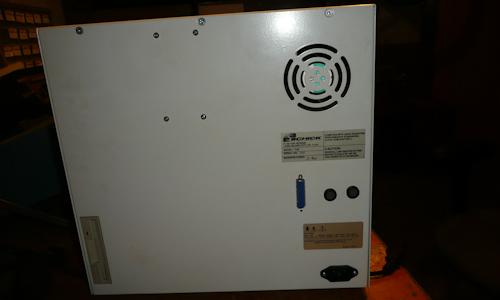
The machine does give you information such as bone thickness and other stuff, all of which is not that relevant to us, but now we know that it has to have a processor capable of analyzing the X-ray image. Not to mention that if it saves a report to a floppy disk which is going to be opened on another computer, it has to have file system drivers. The connector on the back is for connecting to a printer which works with a normal computer using a parallel port, so it also has to have drivers for that. This does not seem like a task for a MCU, but instead for a more full fledged system. So, just from looking at the back of the unit and the user manual, we now know that it has a high voltage supply for the X-ray head, a touchscreen LCD, a floppy disk for storing documents, and probably running an OS of sorts.
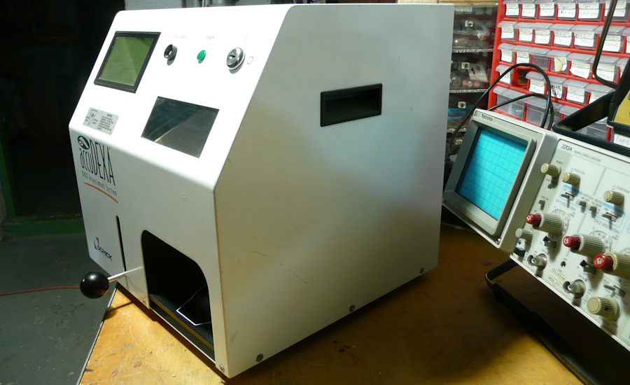
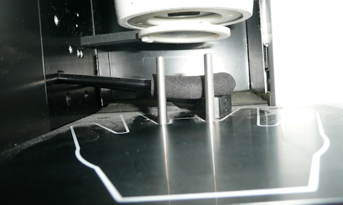
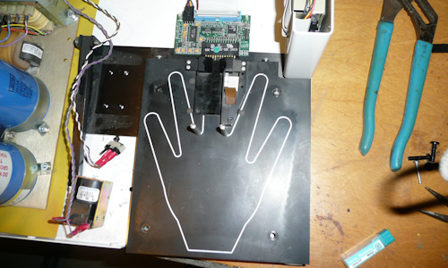
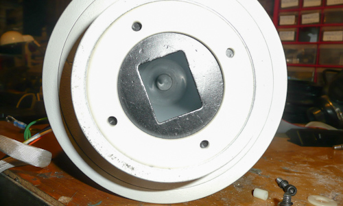
The unit takes two X-ray images of the finger, each with varying strength. At first I would expect it to just vary the strength by changing the voltage to the X-ray head, but I am guessing that instead it was cheaper to just put some metal between the X-ray head and the finger. There is a linear actuator which pushes a lever that the metal disk is attached to, pushing the disk out of the way of the X-ray head. This is explained more on the AccuDexa site in the user manual. The two rods that stick out above the finger are what hold the finger down to prevent movement when taking the X-ray, and the big lever seen earlier is attached to them.
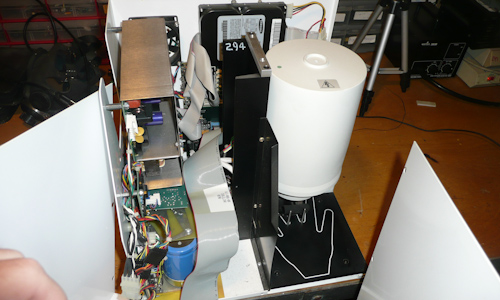
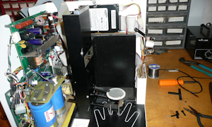
The big lever can be taken off by just unscrewing it, and the screws for the unit are luckily not some security ones. Now, this is surprising. At first glance you can spot the power supply on the top left, two huge capacitors, the big white cylindrical X-ray head, and a hard drive with an IDE cable and a molex power connector. I am starting to think that they just shoved an entire computer into here. But I will restrain myself from pulling it apart even more and instead focus on getting it to power on first.
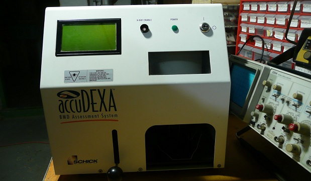
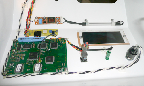
And here is the front of the unit. A small overview of what is what from first glance. The top right square is the slot to put the patients hand into, the slot next to it is where the big lever went. Under that is a rectangular PCB, which is the CCFL driver for the light to the right of it. It takes the low voltage (12v probably) and using a transformer generates hundreds of volts to ignite the CCFL, and then steps to a lower voltage to drive the CCFL.
The PCB under the CCFL driver is a very simple one sided board, no silkscreen or solder mask even, and it has two triacs, though I do not know what it is for, my best guess is contrast and brightness adjustment for the LCD. The very large board under the simple rectangular board is the touchscreen driver, with what I am guessing is a parallel data cable. The cylinder on the right of the touchscreen board is the X-ray indicator, then the power indicator, and lastly the key power switch.
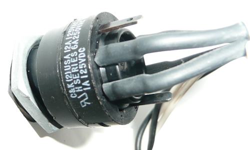
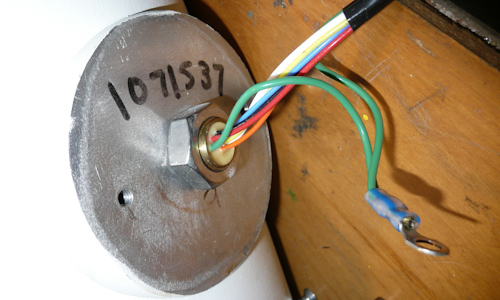
TA closer look at the power switch reveals some identifiers of the key, and that it has four wires. Since they are colored black and white, and seem to have thick insulation, I am guessing that it is carrying mains, not to mention the heat shrink over the connectors to the key switch. A look at the datasheet of the switch gives us some good information, though I was unable to find the same model as the one in front of me. Since I was unable to find the pin out, and I do not have any heat shrink on hand, I decided to try and just take it apart, forcing it into the on position.
Motivation provided by the data sheet saying "Switch installation is permanent. Switch cannot be removed from lock after assembly."
After some mucking around, I managed to force open the switch assembly, and turn the switch into the "on" position. Now, to put it back together …
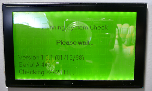
It works! Awesome! Nothing seems to be melting, smoking, or catching fire, which is all very good news! Looking at some of the files it is checking, I am guessing it runs MS-DOS or windows CE or something of the sort. Though, look at the date! 1998! This machine is extremely old, probably cost a fortune back then.
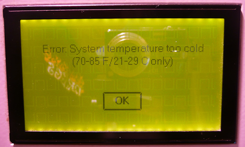
Everything was going far too well, back to equilibrium now. The temperature in the basement is indeed within the specified temperature range given on the screen, but it does not seem to matter for the machine. The manual says to let the machine sit in the correct temperature range for a few hours before turning on, and the machine has been in that room for nearly a full 24 hours, so I am guessing it was thrown out for a few reasons, including that the temperature sensor does not work, not to mention how old the unit is. I would hope that there have been some advances in medical X-ray technology in the past 14 years to warrant the purchase of a new machine. Oh well, time to take it apart and find the sensor.
A quick google does not give me anything on either of those two stickers, but there is not much to see on such an LCD controller board. It probably has a few chips to drive the screen itself, then the main controller that handles the data going in and out, some RAM for the screen, and a flash storage chip for containing the different characters and images. To get a good write up of such a board it would warrant another tear down just for itself. The wire going to the middle of the board that looks glued on is from the very simple rectangular PCB earlier, so I think I am right in thinking that the function of it is for contrast and brightness.
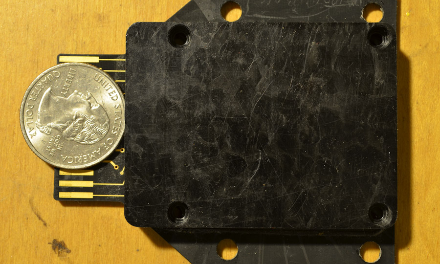
Close up of the super simple rectangular board.
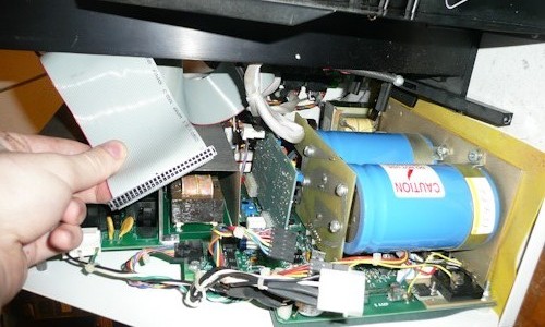
And here is where it gets interesting. What you are seeing is the power modules for the entire xray machine. The blue cylinders on the bottom are what I am guessing, smoothing capacitors for the AC to DC rectification. When current demands rise in a rectified load, you need larger smoothing capacitors so when the current is drawn towards the end or beginning of the cycle, it comes from the capacitors which stored current from the middle-ish of the cycle. If you want to learn more, google "smoothing capacitors" for a better explanation, as I know mine sucks quite bad. The cable I am holding goes from somewhere behind the X-ray head to the touchscreen in the front panel.
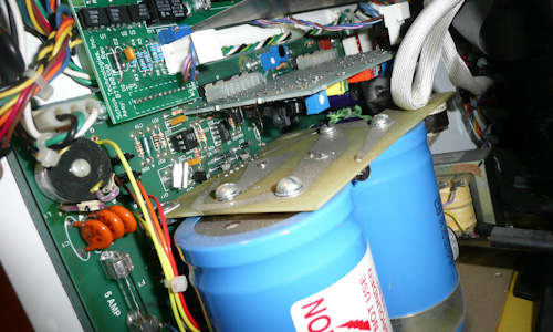
Another angle of the power section of the unit. In the left most side of the picture, you can spot the white and black cables seen earlier, a fuse, and an EMI filter of sorts. These guys are all between the mains and the rectification, always, and since this is a unit that draws so much power (700 watts I believe), the diode bridge must be on some large heat sink of sorts, unless it is attached to the case, which would be very dangerous to do.
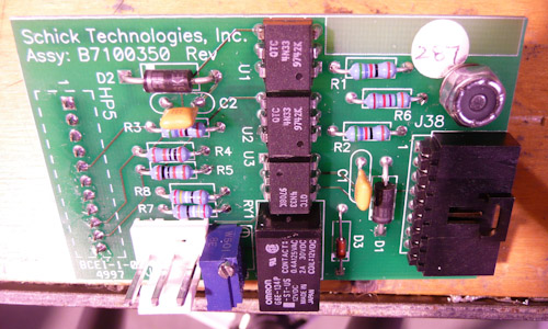
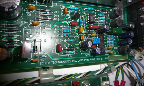
Here is one of the boards seen within the power section of the unit. We see a trimmer potentiometer, a relay rated for 2A at 30V (boxes shaped like this on a board are almost always relays), and some ICs. They are photodarlingtons, otherwise known as opto-isolators, usually used for isolation between high voltage (mains or primary side of step down power supply), with a line under them indicating the separation of the high voltage and low voltage sides of the board. In this case there is no such line drawn, but usually there is. They are 4N33 made in the year 1997, in the eight week and 42nd week, as shown by the date code 9708 and 9742
The component side of another board, this one being directly connected to one of the power supply boards. It has some really cool test points, with the colors and plastic covers. I wonder why they did it like that and not just what you see today, which is a tiny copper pad used with a "bed of nails", which I think they should have had back then. Also, notice that one of the traces are a right angle instead of thhe usual 45 degree bends we see nowadays. From what I understand, it is due to manufacturing that the bends are like that, specifically with how the enchant eats away at the copper, and if you have such a 90 degree bends the chances of the etching process going bad at the bend are rather high. If interested, here are some Full size closeups of the board, component side.
Picture 1
Picture 2
Picture 3
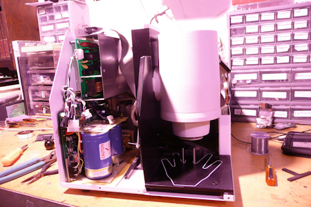
Here is what the machine looks like so far. Time to take the huge X-ray head off!
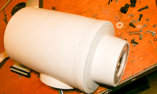
The X-ray head is attached the machine using a hex screw, and I only have the long hex screwdrivers, so after quite a bit of mucking around trying to unscrew them in such a small space, I managed to take off the X-ray head. I have to say, the X-ray head is rather heavy, and when you knock on it then it sounds "full". One of my possible explanations, is that in the user manual it says that the X-ray head is oil cooled, with a maximum anode power of 700 watts, so I guess that the X-ray head is an enclosed system, including the liquid cooling, voltage multiplier, and the high voltage transformer. There is a lack of any fins, so I am guessing that the outer metal is a "shell", with the oil flowing near the surface, allowing heat to be released that way. There are no heavily insulated wires, and no tubes going to the X-ray head, so I am guessing that this is the case. My other idea is that it is just really thick metal, but it may be both.
The only identification marks I can find on the X-ray head. A short google sadly does not find me anything.
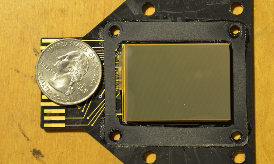
Taking off the black metal surrounding the X-ray "area" gives me this. I am guessing the black metal acts as shielding, but I am not sure. Here you can spot the place to put the hand, the finger, and a board with some wires. This is where the X-ray camera resides.
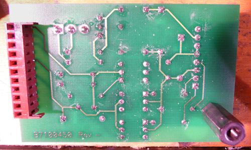
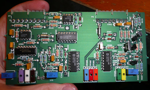
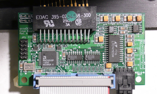
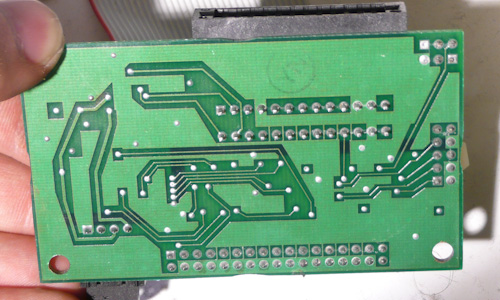
A closer look reveals a few logic chips, such as the MM74HC157M, a multiplexor, a MACH211SP, which is a programable logic device, and a LTC1415CSW, which is a 12 bit, 1.25 MSPS ADC, with a parallel data output.
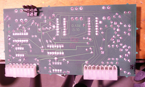
And this is the back of that board.
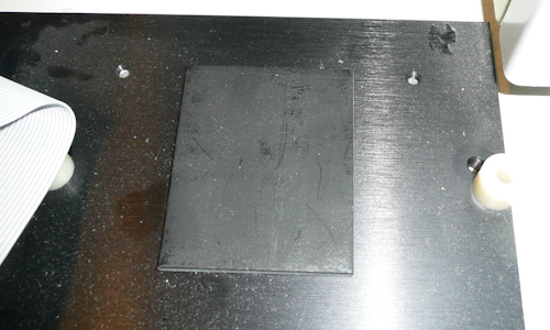
After taking off the X-ray "camera", the plate that provides calibration and testing for the X-ray according to the user manual can now be seen. From what I understand, it provides very good contrast against the bone of the finger.
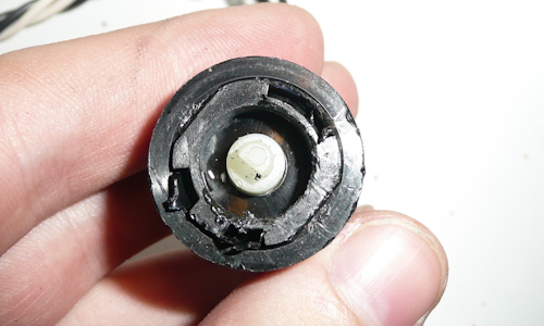
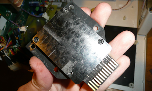
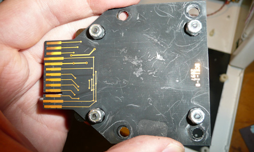
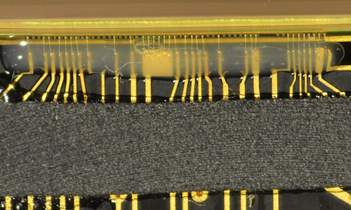
The X-ray sensor seems rather simple, but I cannot seem to open it, even after unscrewing the screws holding it together. I am thinking that inside there may be another gas or something like that, hence them gluing it shut after screwing it shut, so before going any further I will ask the awesome people at 4HV for any ideas, and if there is anything dangerous possibly lurking there.
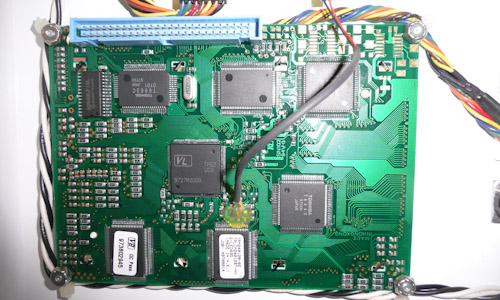
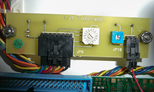
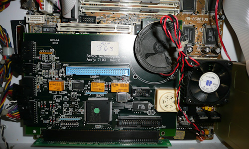
After a while it looks like they just put in an entire computer, but to get to out I have to get through this ISA card. Some chips on it that I see are the IDT72403L35SO, a FIFO, a MACH5 CPLD, some relays, a buzzer, speaker, and some logic ICs. The board is attached to the motherboard of the computer with some screws, one of which was behind the speaker, which was attached to the PCB way off center.
Frustrating screw
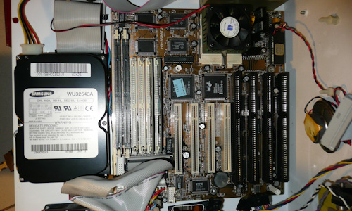
And here is most of the computer, excluding the card I took out earlier. It has a blazing fast Pentium 2 with no thermal paste, a whopping 64MB of ram it seems, and about a 2GB HDD.
Part of the top power board, specifically the maker of the board.
The wiring from the xray head, with some sort of potting material. I would really want to check out the xray head, especially the high voltage components, but before I try to disassemble the X-ray head, I will ask the community at 4hv if there is anything that might pose a risk to anyone.
And a final picture showing an idea of the size of the X-ray head.
