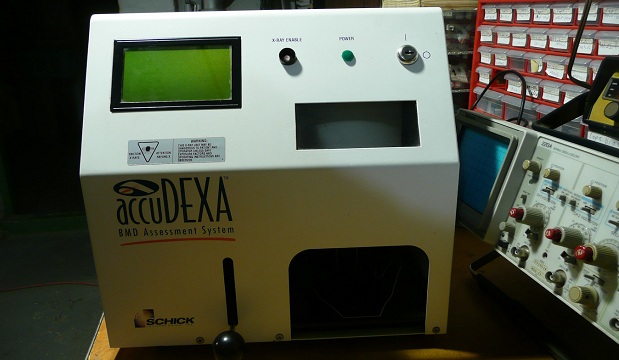
It did not require much force to open the sensor, and much to my surprise, the size of the sensor is huge. The way this sensor works is the x-rays from the x-ray head pass through items that do not absorb or block x-rays, such as skin and other body tissues, showing a negative of the bone. The x-rays which made it through the finger pass through the plastic case of the sensor easily, hitting a screen that "converts" the x-rays into visible light, known as a scintillator, which then hits the sensor generating an analog value for each pixel. If I want to use this sensor, I need to find out how it works, and to do that I need to look at how to sensor is connected to the rest of the system.
Instead of just taking a picture and linking to pictures of boards, I think that it would be better to show the boards via a Google maps like viewer. This way there is not a huge amount of bandwidth wasted when the individual is not interested in a specific part of the image and you can zoom in on the image to your heart’s content. The way this is done is by taking zoomed in pictures of the board in a grid, and then stitching them together, otherwise known as a panorama. Of course, sometimes the stitching does not work out that well, leading to curved images or slightly misaligned stitches.
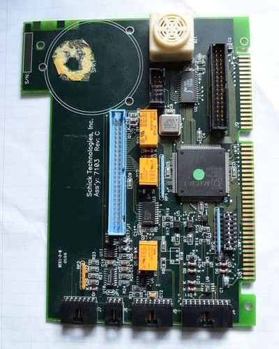
The first image is of the board that connects directly to the x-ray image sensor. Looking closely you can spot a few key features on the board which can help identify its function. Firstly, the left most part of the board has a logic IC, a MACH211SP PDF. It is what you can call a CPLD, sometimes called "glue logic" because they act as small miscellaneous logic that connects other chips together, and it only works with digital signals, 1's and 0's, no analog things go on here. Not to mention, it is from 1997 and has 64 macro cells, so no ADC's or DAC's on CPLD's back then, it was either all digital or all analog, rarely both on the same die.
Before going further, one of the most important things when trying to reverse engineer a circuit board is finding out how each component is connected, or in other words, finding out where the traces go on the board. One of the biggest problems that an individual might encounter is when a PCB has more than two layers, because finding out where the traces go on the inside of the PCB is nearly impossible without destroying the board, especially when you have large copper pours on the top and bottom. A good way to tell if a board has more than two layers is either shining a light through and seeing if there is a non-translucent object inside the board, or checking if there are any via's that do not have a connection at the top and bottom layers. Yet another good way to spot a board that has more than two layers is if the top and bottom of the board do not have traces cutting through copper pours on the top and bottom, because, well how else would you connect components on a board with only two layers? In this case, almost all the via's are connected at the top and bottom, leaving no magical unconnected via's, I do not see any copper shadows when shining light through the board, and most traces seem accounted for. One thing that puzzles me though is the amount of unused pins on some of the IC's and very few via's under IC's for power, specifically the CPLD.
Anyways, the other chips on the board are two MM74HC157M's PDF. These are logic IC's, more specifically multiplexors manufactured by National according to the logo on the top left of the chip. When I started to trace how the CPLD is connected with the possible logic IC's, I realized that there are too many unconnected via's, especially with the second 74HC157M to the right, U6, because the VCC pin leads to a via on the top that is not connected anywhere at the bottom via. Also, there are via's that connect the top copper pour to the bottom pour, so both are ground and presumably act as shielding. Another reason they are both ground is because all of the tantalum capacitors are connected to the supposedly ground, copper pours with their negative polarity side. Later on, we can spot that the CPLD has two pins connecting to the select pins for each of the two logic IC's, which control which input (A or B) to put on the output(Y). Their outputs all go to the blue IDE connector on the bottom of the board.
Next up is a LTC1415CSW PDF, a 1.25 MHz 12 bit ADC. Its output is in the form of a 12 bit parallel bus, which leads to the logic chips that function as a multiplexor, taking the 12 bits from the ADC and changing it into 8 bits, which would require two cycles for the full 12 bits to get through. Since the logic IC's are quad multiplexors per chip, and there are two chips, that gives you 8 output bits for 16 input bits, but the ADC is only 12 bits, so the designer set the last four gate inputs as D_IN and GND, like this. Yes I know the drawing is not the best out there.
So now we know that the PCB takes in an analog signal from the actual sensor and takes that to the ADC, which then outputs its value on a 12 bit bus to two IC's, each having four multiplexors. These chips change the one cycle twelve bit value to a two cycle eight bit value. The next board along the way is the connector card that plugs into the motherboards expansion slot, which in this case is an ISA bus. And here I will go off on a little tangent, to demonstrate an essential step that happens to everyone every now and then, and what my thinking process was. When you look at the ISA bus specifications, which you can find from googling for a few seconds, you then realize exactly why the ADC 12 bit single cycle output is changed to a two cycle eight bit signal, the ISA bus has an eight bit data bus, not twelve, not sixteen, only a small eight bits, with the rest of the bus consists of handshaking bits and address bits.
The ISA bus was designed by IBM as a buffer for the external 8 bit data bus for the Intel 8088 processor, hence the bus only having 8 bits for data. In short, the ISA bus was designed originally for the Intel 8088 external bus, so it was planned out with the limitations of the 8088 in mind. Best of all, the bus runs at 4.77 MHz which is more than fast enough, so my theory of the 12 bit to two 8 bit conversion seems to make even more sense. But here is where my mistake happened, a slight overlook of something very basic and obvious. While the bus used by the second card is indeed the ISA bus, and it does have an eight bit data bus, I did not look at which ISA bus is used. There are actually two ISA busses out there, one of which is the eight bit bus which was just looked at, but that is actually a legacy component of the ISA bus.
Since the eight bit ISA bus was originally brought to market for the Intel 8088 in 1981, it was realized that a 16 bit bus would come in handy for the newer Intel 80286 in 1984. When I was looking at the ISA specification, I did not notice that there was a modern sixteen bit and legacy eight bit version of the ISA bus, nor did I notice that the diagram showing the pin-out for the ISA bus had no stubble that existed in the physical card. In short, I did not notice that I was looking at the legacy eight bit legacy version of the ISA bus instead of the newer 16 bit one used for this card. A simple oversight can lead you down the wrong path of verification and explanation, resulting in wasted time and in the end, confusion due to the mixing up of earlier irrelevant information to the now relevant and correct information. Do check that you are using the right version of your busses from time to time.
While I was wrong with my thinking for why there was a conversion from the 12 bit ADC signal to an 8 bit signal, there is still a good reason why the bit count is changed to eight bits, and the answer is obvious when looking closer at what IC's are on this board and tracing where the ribbon cable goes from the X-ray acquisition board. The ribbon cable is connected to the connector on the bottom right of the board, under the buzzer. Let’s look at that chip right above the connector, since we see that four traces go directly to the IC from the connector, and there are four VIA's right under the chip, which would add up to the eight bits that we are getting so familiar with.
Searching for just "L35SO" does not give us anything meaningful, nor do any of the other items on the chip, not even the "DT". When you look closer, you can tell that the bottom numbers are the date the IC was manufactures, the 36th week of 1997, so that obviously is not what we are looking for. Since searching using the remaining two phrases does not give us anything, combining them is worth a shot, and lo and behold it does give us something when we search for L204L35SO, and the company name is actually IDT. Since the "I" in the IDT logo on the chip looks like the most unusual "I" I have ever seen, I ended up originally searching for the company name using just "DT", obviously not finding anything.
The L204L35SO is a FIFO, or a first in first out memory IC, in this case acting as a buffer. An analog signal enters the ADC, which generates a 12 bit signal at 1.25 MHz. The 1.25 MHz 12 bit signal gets converted into a 2.5 MHz 8 bit signal, which travels through the ribbon cable to this board. Here is why we have a FIFO; the ISA bus introduces unpredictable latency. The ISA bus on the motherboard is used by other components, such as a sound card or modem, so all other items on the ISA bus have to compete for access to the bus, resulting in some components getting access at a later time then would be most optimal, generating a queue so to speak. The card cannot have access for the duration of the entire image capture all in one go, so while the card is waiting for the ISA bus, the data is stored in this FIFO.
This is why there is a FIFO here, it acts as a buffer for data from the ADC, and when the card gets access to the ISA bus the data will flow out of the FIFO and then fill up again. Also, the FIFO is only about 4096 bytes large, so if each pixel in the sensor takes 16 bits, or two bytes, that would mean that the FIFO can hold 2048 pixels, which is probably enough to hold the entire X-ray image.
The IC to the left of the FIFO is a Mach 5 128 CPLD from AMD. Yes, AMD used to make chips that were not just graphics and processors like they do today. It is a chip that you can consider as a very large amount of logic gates (5,000 ish in this case) that you can program individually. Also, it is 500 nm! A very far cry from today's I5's based on 32nm, the FX-8150 based on also 32nm, and the upcoming Haswell based on 22 nm.
Anyways, this chip is used as the transceiver, meaning it takes the data buildup from the FIFO and sends it to the ISA bus, handling the addressing, handshaking, and all the other goodies associated with a very large bus. The little switches on the left of the CPLD serve as configuration bits, but that is all you can really tell without delving into the Verilog or VHDL used for programming the CPLD. All the other connectors to the left of the board are connected to a very large power board, and a few other boards inside the X-ray unit.
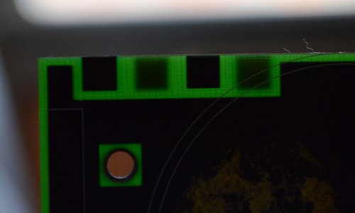
Building on how I explained earlier the signs of a four or more layer board, this is a good example of a board with more than just two layers. The left most square is actually greenish, indicating copper, and the 2nd square from the right is the silk screen. The top layer silk screen and copper each have a small square to allow the designer to keep track of what layer goes where when the PCB is manufactured, though it is done rarely these days, especially with boards that have eight or more layers. Each layer has its own silk screen and copper square, hence having four squares that light does not pass through. And lastly, another good way to tell this board has more than two layers would be VIA's that do not connect to anywhere on both the top and layers at the same time. Considering these via's normally go from what seems to be decoupling capacitors, chances are they go to the ground and power planes in the second and third layers.
Page 1
TO BE CONTINUED
